拓扑与架构
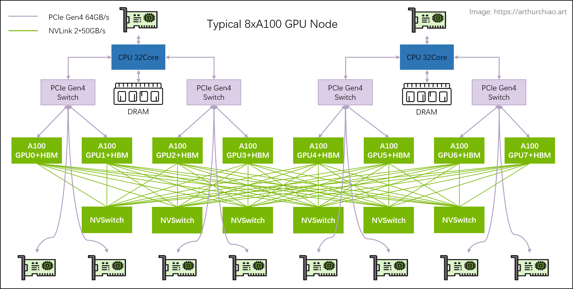
PCIe 架构
NVLink
NVLink is a wire-based serial multi-lane near-range communications link developed by Nvidia. Unlike PCI Express, a device can consist of multiple NVLinks, and devices use mesh networking to communicate instead of a central hub. The protocol was first announced in March 2014 and uses a proprietary high-speed signaling interconnect (NVHS).
简单总结:同主机内不同 GPU 之间的一种高速互联方式,
- 是一种短距离通信链路,保证包的成功传输,更高性能,替代 PCIe,
- 支持多 lane,link 带宽随 lane 数量线性增长,
- 同一台 node 内的 GPU 通过 NVLink 以 ==full-mesh== 方式(类似 spine-leaf)互联,
- NVIDIA 专利技术。
演进:1/2/3/4 代
主要区别是单条 NVLink 链路的 ==lane 数量==、每个 ==lane 的带宽==(图中给的都是双向带宽)等:
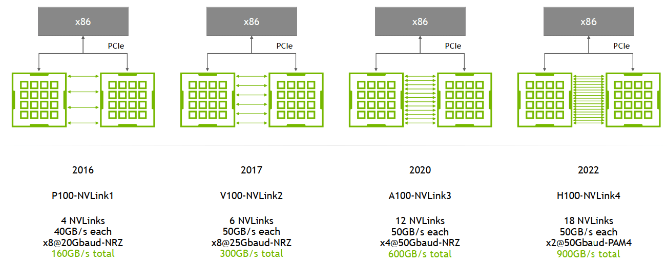
例如,
-
A100 是 ==
12 lane * 50GB/s/lane = 600GB/s== 双向带宽(单向 300GB/s) -
A800 被阉割了 4 条 lane,所以是 ==
8 lane * 50GB/s/lane = 400GB/s== 双向带宽(单向 200GB/s) -
Pascal 的 Nvlink1.0的 IO 速率是20Gbps,8 Lane per Port,每个 Port 320Gbps(双向),这其实是一代不完全成熟的产品,因为这个 Port 的速率很独特,GPGPU 内部微架构团队可能也还没有完全接纳。
-
Volta的Nvlink2.0的IO速率是25Gbps,8Lane per Port,每个Port 400Gbps(双向),从此时开始,GPGPU对这个数字就锁定了。
-
Ampere的Nvlink3.0的IO速率是50Gbps,4Lane per Port,每个Port 400Gbps(双向)。
-
Hopper的Nvlink4.0的IO速率是100Gbps,2Lane per Port,每个Port 400Gbps(双向)。
-
Blackwill 的 Nvlink5.0,没发布,但以此类推,大致就是 IO 速率200Gbps,1Lane per Port,每个 Port 400Gbps
问题,这里的 lane, port 以及 NVLink 之间的定义
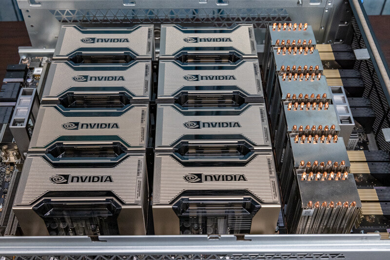
NVSwitch
NVSwitch 是 NVIDIA 的一款**==交换芯片==,封装在 GPU module 上,并==不是主机外的独立交换机==**。
下面是真机图1,浪潮的机器,图中 8 个盒子就是 8 片 A100,右边的 6 块超厚散热片下面就是 NVSwitch 芯片:
NVLink Switch
==NVSwitch == 听名字像是交换机,但实际上是 GPU module 上的交换芯片,用来**==连接同一台主机内的 GPU==**。
2022 年,NVIDIA 把这块芯片拿出来真的做成了交换机,叫 ==NVLink Switch == 2,用来**==跨主机连接 GPU 设备==**。
这俩名字很容易让人混淆。
https://www.nvidia.com/en-us/data-center/nvlink/ 有个视频讲的很清楚
NVLink Network
On top of fourth-generation NVLink, H 100 also introduces the new NVLink Network interconnect, a scalable version of NVLink that enables GPU-to-GPU communication among up to 256 GPUs across multiple compute nodes.
Unlike regular NVLink, where all GPUs share a common address space and requests are routed directly using GPU physical addresses, NVLink Network introduces a new network address space. It is supported by new address translation hardware in H 100 to isolate all GPU address spaces from one another and from the network address space. This enables NVLink Network to scale securely to larger numbers of GPUs.
Because NVLink Network endpoints do not share a common memory address space, NVLink Network connections are not automatically established across the entire system. Instead, similar to other networking interfaces such as InfiniBand, the user software should explicitly establish connections between endpoints as needed.
HBM
演进:HBM 1/2/2e/3/3e
From wikipedia HBM,
| Bandwidth | Year | GPU | |
|---|---|---|---|
| HBM | 128GB/s/package | ||
| HBM2 | 256GB/s/package | 2016 | V100 |
| HBM2e | ~450GB/s | 2018 | A100, ~2TB/s, |
| HBM3 | 600GB/s/site | 2020 | H100, 3.35TB/s |
| HBM3e | ~1TB/s | 2023 | |
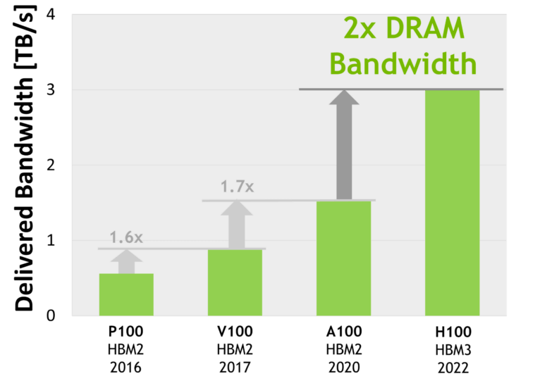
使用了 HBM 的近几代高端 NVIDIA GPU ==显存带宽==(双向),纵坐标是 TB/s。Image source: [3]
- AMD MI300X 采用 192GB HBM3 方案,带宽 ==
5.2TB/s==; - HBM3e 是 HBM3 的增强版,速度从 6.4GT/s 到 8GT/s。预计 2024 量产。
Reference
-
No backlinks found.